博文目录
- 写在前面
- 正文
- 赋值语法
- reg类型变量赋值
- 隐性连续赋值
- 组合逻辑设计
- 举例说明
- 参考资料
- 交个朋友
写在前面
本系列相关博文链接:
Verilog初级教程(7)Verilog模块例化以及悬空端口的处理
Verilog初级教程(6)Verilog模块与端口
Verilog初级教程(5)Verilog中的多维数组和存储器
Verilog初级教程(4)Verilog中的标量与向量
Verilog初级教程(3)Verilog 数据类型
Verilog初级教程(2)Verilog HDL的初级语法
Verilog初级教程(1)认识 Verilog HDL
芯片设计抽象层及其设计风格
Verilog以及VHDL所倡导的的代码准则
FPGA/ASIC初学者应该学习Verilog还是VHDL?
-
个人微信公众号: FPGA LAB
-
个人博客首页
-
注:学习交流使用!
正文
wire类型的信号需要连续赋值。例如,考虑一根电线用于连接面包板上的元件。只要将+5V电池施加在电线的一端,连接在电线另一端的元件就会得到所需的电压。

在Verilog中,这个概念是通过赋值语句(assign)来实现的,在赋值语句中,任何线或其他类似线的数据类型都可以用一个值来连续驱动,这个值可以是常数,也可以是一组信号组成的表达式。
赋值语法
赋值语法以关键字assign开头,后面是信号名,可以是单个信号,也可以是不同信号网的连接。驱动强度和延迟是可选的,主要用于数据流建模,而不是综合到实际硬件中。右侧的表达式或信号被分配给左侧的网或网的表达式。
语法结构如下:
assign <net_expression> = [drive_strength] [delay] <expression of different signals or constant value>
延迟值对于指定门的延迟很有用,并用于模拟实际硬件中的时序行为,因为该值决定了何时应该用评估值分配网。
使用 assign 语句时, 需要遵循一些规则:
- LHS(左值) 应该始终是wire类型的标量或向量网络, 或者标量或矢量网络的串联, 而绝对不能是reg类型的标量或矢量寄存器。
- RHS 可以包含标量或向量寄存器以及函数调用。
- 只要 RHS 上的任何操作数的值发生变化, LHS 就会使用新值进行更新。
- assign 语句也称为连续赋值, 并且始终处于活动状态
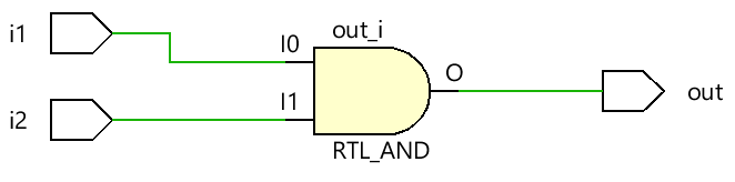
例如:

综合后的RTL图:
reg类型变量赋值
reg类型的变量不能使用assign进行连续赋值,这是因为reg类型的变量可以存储数据,并且不需要连续驱动。我们只能在initial以及always块内对reg类型变量进行赋值。
隐性连续赋值
当使用assign给wire类型的网络赋值时,称为显示连续赋值,如果在定义的时候就对其连续赋值,称为隐形连续赋值。
wire [1:0] a;
assign a = x & y;       // Explicit assignmentwire [1:0] a = x & y;   // Implicit assignment
隐形连续赋值在Verilog中是被允许的。
组合逻辑设计
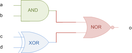
assign语句常用于组合逻辑设计,如下的电路图:

使用Verilog描述为:
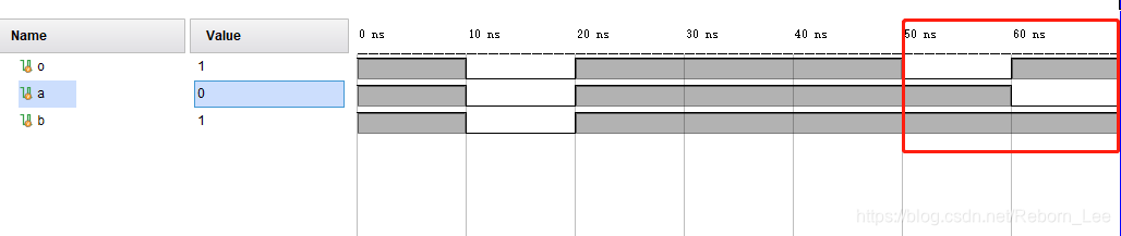
// This module takes four inputs and performs a boolean
// operation and assigns output to o. The combinational
// logic is realized using assign statement.module combo (  input   a, b, c, d,output  o);assign o = ~((a & b) | c ^ d);endmodule
其RTL硬件原理图为:

行为仿真:

举例说明
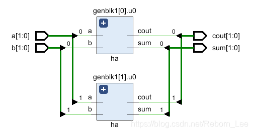
半加器设计
Verilog描述为:
module ha ( input   a, b,output  sum, cout);assign sum  = a ^ b;assign cout = a & b;
endmodule
对应的RTL原理图为:

tb文件:
module tb;// Declare testbench variablesreg a, b;wire sum, cout;integer i;// Instantiate the design and connect design inputs/outputs withha u0 ( .a(a), .b(b), .sum(sum), .cout(cout));initial begin// At the beginning of time, initialize all inputs of the design// to a known value, in this case we have chosen it to be 0.  a <= 0;b <= 0;// Use a $monitor task to print any change in the signal to // simulation console     $monitor("a=%0b b=%0b sum=%0b cout=%0b", a, b, sum, cout);// Because there are only 2 inputs, there can be 4 different input combinations// So use an iterator "i" to increment from 0 to 4 and assign the value// to testbench variables so that it drives the design inputs    for (i = 0; i < 4; i = i + 1) begin{a, b} = i;#10;endend
endmodule
仿真结果:
ncsim> run
a=0 b=0 sum=0 cout=0
a=0 b=1 sum=1 cout=0
a=1 b=0 sum=1 cout=0
a=1 b=1 sum=0 cout=1
ncsim: *W,RNQUIE: Simulation is complete.

更多的例子不在话下。
参考资料
- 参考资料1
- 参考资料2
交个朋友
-
个人微信公众号:FPGA LAB
-
知乎:李锐博恩
-
FPGA/IC技术交流2020