文章目录
- 17.集成电路
- 真空管时代
- 晶体管时代
- 集成电路时代
- 印刷电路板时代
- 光刻时代
17.集成电路
Over the past six episodes, we delved into software,
过去 6 集我们聊了软件 \N 从早期编程方式到现代软件工程
from early programming efforts to modern software engineering practices.
Within about 50 years, software grew in complexity from machine code punched by hand onto paper tape
在大概50年里 软件从纸带打孔 \N 变成面向对象编程语言 在集成开发环境中写程序
to object oriented programming languages, compiled in integrated development environments.
But this growth in sophistication would not have been possible without improvements in hardware.
但如果没有硬件的大幅度进步 \N 软件是不可能做到这些的
真空管时代
To appreciate computing hardware’s explosive growth in power and sophistication,
为了体会硬件性能的爆炸性增长 \N 我们要回到电子计算机的诞生年代
we need to go back to the birth of electronic computing.
From roughly the 1940’s through the mid-1960s, every computer was built from individual parts,
大约 1940年代~1960年代中期这段时间里 \N 计算机都由独立部件组成
called discrete components, which were all wired together.
叫"分立元件" \N 然后不同组件再用线连在一起
For example, the ENIAC, consisted of more than 17,000 vacuum tubes, 70,000 resistors,
举例, ENIAC 有1万7千多个真空管, 7万个电阻
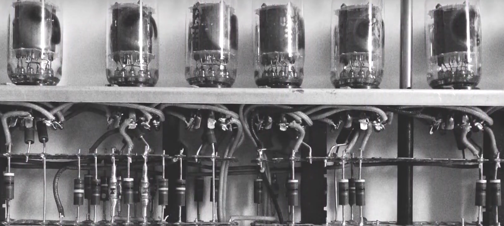
10,000 capacitors, and 7,000 diodes, all of which required 5 million hand-soldered connections.
1万个电容器, 7千个二极管, 5百万个手工焊点
Adding more components to increase performance meant more connections, more wires
如果想提升性能,就要加更多部件 \N 这导致更多电线,更复杂
and just more complexity, what was dubbed the Tyranny of Numbers.
这个问题叫 "数字暴政’’
晶体管时代
By the mid 1950s, transistors were becoming commercially available
1950 年代中期,晶体管开始商业化(市场上买得到) \N 开始用在计算机里
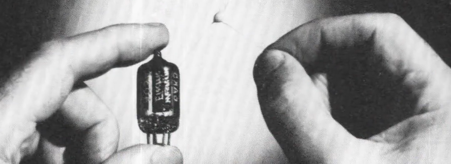
and being incorporated into computers.
These were much smaller, faster and more reliable than vacuum tubes
晶体管比电子管 更小更快更可靠
but each transistor was still one discrete component.
但晶体管依然是分立元件
In 1959, IBM upgraded their vacuum-tube-based “709” computers to transistors by replacing
1959年,IBM 把 709 计算机从原本的电子管 \N 全部换成晶体管
by replacing all the discrete vacuum tubes with discrete transistors.
The new machine, the IBM 7090, was six times faster and half the cost.
诞生的新机器 IBM 7090 \N 速度快 6 倍,价格只有一半
These transistorized computers marked the second generation of electronic computing.
晶体管标志着"计算 2.0 时代"的到来
However, although faster and smaller,
虽然更快更小 \N 但晶体管的出现 还是没有解决"数字暴政"的问题
discrete transistors didn’t solve the Tyranny of Numbers.
It was getting unwieldy to design,
有几十万个独立元件的计算机不但难设计 \N 而且难生产
let alone physically manufacture computers with hundreds of thousands of individual components.
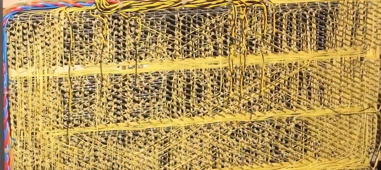
By the the 1960s, this was reaching a breaking point.
1960 年代,这个问题的严重性达到顶点 \N 电脑内部常常一大堆电线缠绕在一起
The insides of computers were often just huge tangles of wires.
Just look at what the inside of a PDP-8 from 1965 looked like!
看看这个 1965 年 PDP-8 计算机的内部
The answer was to bump up a new level of abstraction, and package up underlying complexity!
解决办法是引入一层新抽象,封装复杂性
The breakthrough came in 1958, when Jack Kilby, working at Texas Instruments,
突破性进展在 1958 年 \N 当时 Jack Killby 在德州仪器工作
demonstrated such an electronic part, "wherein all the components of the electronic circuit are completely integrated.
演示了一个电子部件:\N “电路的所有组件都集成在一起”
Put simply: instead of building computer parts out of many discrete components
简单说就是:\N 与其把多个独立部件用电线连起来,拼装出计算机
集成电路时代
and wiring them all together,
you put many components together, inside of a new, single component.
我们把多个组件包在一起,变成一个新的独立组件
These are called Integrated Circuits, or ICs.
这就是 集成电路(IC)
A few months later in 1959, Fairchild Semiconductor, lead by Robert Noyce, made ICs practical.
几个月后,在1959年 Robert Noyce 的仙童半导体 \N 让集成电路变为现实
Kilby built his ICs out of germanium, a rare and unstable material.
Kilby 用锗来做集成电路,锗很稀少而且不稳定
But, Fairchild used the abundant silicon, which makes up about a quarter of the earth’s crust!
仙童半导体公司用硅 \N 硅的蕴藏量丰富,占地壳四分之一
It’s also more stable, therefore more reliable.
也更稳定可靠
For this reason, Noyce is widely regarded as the father of modern ICs,
所以 Noyce 被公认为现代集成电路之父
ushering in the electronics era… and also Silicon Valley, where Fairchild was based
开创了电子时代,创造了硅谷(仙童公司所在地)
and where many other semiconductor companies would soon pop up.
之后有很多半导体企业都出现在硅谷
In the early days, an IC might only contain a simple circuit with just a few transistors,
起初,一个 IC 只有几个晶体管 \N 例如这块早期样品,由西屋公司制造
like this early Westinghouse example.
But even this allowed simple circuits, like the logic gates from Episode 3,
即使只有几个晶体管 \N 也可以把简单电路,第 3 集的逻辑门,能封装成单独组件
to be packaged up into a single component.
ICs are sort of like lego for computer engineers
IC 就像电脑工程师的乐高积木 \N 可以组合出无数种设计
“building blocks” that can be arranged into an infinite array of possible designs.
IC 就像电脑工程师的乐高积木 \N 可以组合出无数种设计
However, they still have to be wired together at some point
但最终还是需要连起来, \N 创造更大更复杂的电路,比如整个计算机
to create even bigger and more complex circuits, like a whole computer.
但最终还是需要连起来, \N 创造更大更复杂的电路,比如整个计算机
印刷电路板时代
For this, engineers had another innovation: printed circuit boards, or PCB
所以工程师们再度创新:印刷电路板,简称 PCB
Instead of soldering and bundling up bazillions of wires, PCBs, which could be mass manufactured,
PCB 可以大规模生产,无需焊接或用一大堆线. \N 它通过蚀刻金属线的方式,把零件连接到一起
have all the metal wires etched right into them to connect components together.
By using PCBs and ICs together, one could achieve exactly the same functional circuit
把 PCB 和 IC 结合使用 \N 可以大幅减少独立组件和电线,但做到相同的功能
as that made from discrete components,
but with far fewer individual components and tangled wires.
Plus, it’s smaller, cheaper and more reliable.
而且更小,更便宜,更可靠. 三赢!
Triple win!
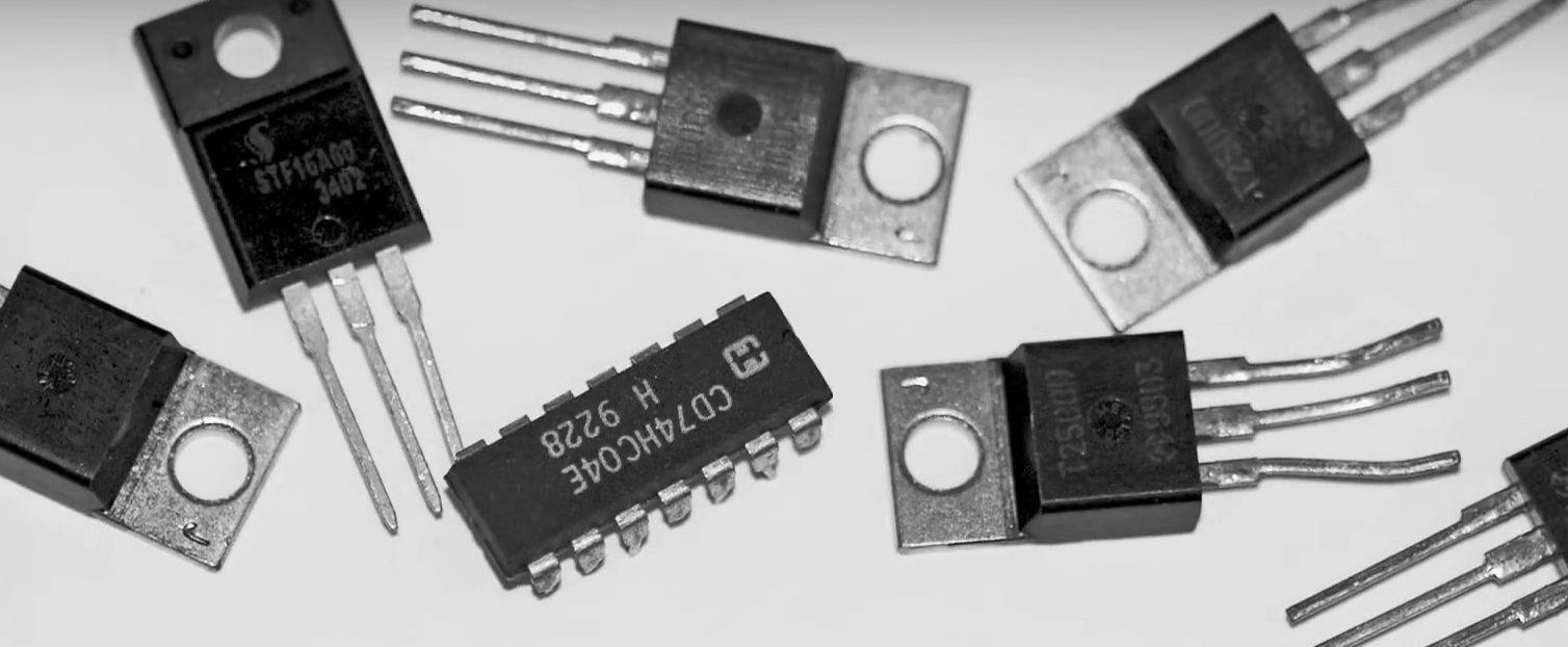
Many early ICs were manufactured using teeny tiny discrete components
许多早期 IC 都是把很小的分立元件 \N 封装成一个独立单元,例如这块 1964 年的IBM样品
packaged up as a single unit, like this IBM example from 1964.
However, even when using really really itty-bitty components,
不过,即使组件很小 \N 塞5个以上的晶体管还是很困难
it was hard to get much more than around five transistors onto a single IC.
光刻时代
To achieve more complex designs, a radically different fabrication process was needed that
为了实现更复杂的设计,需要全新的制作工艺 \N "光刻"登场!
changed everything: Photolithography!
In short, it’s a way to use light to transfer complex patterns to a material, like a semiconductor
简单说就是 \N用光把复杂图案印到材料上,比如半导体
It only has a few basic operations, but these can be used to create incredibly complex circuits.
它只有几个基础操作,但可以制作出复杂电路
Let’s walk through a simple, although extensive example, to make one of these!
下面用一个简单例子,来做一片这个!
We start with a slice of silicon, which, like a thin cookie, is called a wafer.
我们从一片硅开始,叫"晶圆" \N 长得像薄饼干一样
Delicious!
美味!
Silicon, as we discussed briefly in episode 2, is special because it’s a semiconductor,
我们在第 2 集讨论过 \N 硅很特别,它是半导体
that is, a material that can sometimes conduct electricity and other times does not.
它有时导电,有时不导电 \N 我们可以控制导电时机
We can control where and when this happens,
它有时导电,有时不导电 \N 我们可以控制导电时机
making Silicon the perfect raw material for making transistors.
所以硅是做晶体管的绝佳材料
We can also use a wafer as a base to lay down complex metal circuits, so everything is integrated,
我们可以用晶圆做基础 \N 把复杂金属电路放上面,集成所有东西
perfect for… integrated circuits!
非常适合做… 集成电路!
The next step is to add a thin oxide layer on top of the silicon,
下一步是在硅片顶部 \N 加一层薄薄的氧化层, 作为保护层
which acts as a protective coating.
下一步是在硅片顶部 \N 加一层薄薄的氧化层, 作为保护层
Then, we apply a special chemical called a photoresist.
然后加一层特殊化学品, 叫 “光刻胶” \N 光刻胶被光照射后 会变得可溶
When exposed to light, the chemical changes, and becomes soluble,
然后加一层特殊化学品, 叫 “光刻胶” \N 光刻胶被光照射后 会变得可溶
so it can be washed away with a different special chemical.
可以用一种特殊化学药剂洗掉
Photoresists aren’t very useful by themselves,
单单光刻胶本身,并不是很有用 \N 但和"光掩膜"配合使用会很强大
but are super powerful when used in conjunction with a photomask.
单单光刻胶本身,并不是很有用 \N 但和"光掩膜"配合使用会很强大
This is just like a piece of photographic film, but instead of a photo of
光掩膜就像胶片一样,只不过不是 \N 吃墨西哥卷饼的可爱仓鼠,而是要转移到晶圆上的图案
a hamster eating a tiny burrito, it contains a pattern to be transferred onto the wafer.
光掩膜就像胶片一样,只不过不是 \N 吃墨西哥卷饼的可爱仓鼠,而是要转移到晶圆上的图案
We do this by putting a photomask over the wafer, and turning on a powerful light.
把光掩膜盖到晶圆上,用强光照射 \N 挡住光的地方,光刻胶不会变化
Where the mask blocks the light, the photoresist is unchanged.
把光掩膜盖到晶圆上,用强光照射 \N 挡住光的地方,光刻胶不会变化
But where the light does hit the photoresist it changes chemically ,
光照到的地方,光刻胶会发生化学变化 \N 洗掉它之后,暴露出氧化层
which lets us wash away only the photoresist that was exposed to light, selectively revealing areas of our oxide layer.
光照到的地方,光刻胶会发生化学变化 \N 洗掉它之后,暴露出氧化层
Now, by using another special chemical, often an acid, we can remove any exposed oxide,
用另一种化学物质 - 通常是一种酸 \N 可以洗掉"氧化层"露出的部分, 蚀刻到硅层
and etch a little hole the entire way down to the raw silicon.
用另一种化学物质 - 通常是一种酸 \N 可以洗掉"氧化层"露出的部分, 蚀刻到硅层
Note that the oxide layer under the photoresist is protected.
注意,氧化层被光刻胶保护住了.
To clean up, we use yet another special chemical that washes away any remaining photoresist.
为了清理光刻胶,我们用另一种化学药品洗掉它
Yep, there are a lot of special chemicals in photolithography,
是的,光刻法用很多化学品,每种都有特定用途
each with a very specific function!
是的,光刻法用很多化学品,每种都有特定用途
So now we can see the silicon again,
现在硅又露出来了 \N 我们想修改硅露出来的区域 让它导电性更好
we want to modify only the exposed areas to better conduct electricity.
现在硅又露出来了 \N 我们想修改硅露出来的区域 让它导电性更好
To do that, we need to change it chemically through a process called: doping.
所以用一种化学过程来改变它,叫"掺杂"
I’m not even going to make a joke. Let’s move on.
不是开玩笑!我们继续
Most often this is done with a high temperature gas, something like Phosphorus,
“掺杂” 通常用高温气体来做,比如磷 \N 渗透进暴露出的硅,改变电学性质
which penetrates into the exposed area of silicon.
“掺杂” 通常用高温气体来做,比如磷 \N 渗透进暴露出的硅,改变电学性质
This alters its electrical properties.
“掺杂” 通常用高温气体来做,比如磷 \N 渗透进暴露出的硅,改变电学性质
We’re not going to wade into the physics and chemistry of semiconductors,
半导体的具体物理和化学性质我们不会深究,
but if you’re interested, there’s a link in the description to an excellent video
如果你感兴趣,描述里有个视频链接 \N 视频制作者是 Derek Muller 他的频道叫 Veritasium
by our friend Derek Muller from Veritasium.
如果你感兴趣,描述里有个视频链接 \N 视频制作者是 Derek Muller 他的频道叫 Veritasium
But, we still need a few more rounds of photolithography to build a transistor.
但我们还需要几轮光刻法 来做晶体管
The process essentially starts again, first by building up a fresh oxide layer …
过程基本一样,先盖氧化层,再盖光刻胶
which we coat in photoresist.
过程基本一样,先盖氧化层,再盖光刻胶
Now, we use a photomask with a new and different pattern,
然后用新的光掩膜,这次图案不同 \N 在掺杂区域上方开一个缺口
allowing us to open a small window above the doped area.
然后用新的光掩膜,这次图案不同 \N 在掺杂区域上方开一个缺口
Once again, we wash away remaining photoresist.
洗掉光刻胶
Now we dope, and avoid telling a hilarious joke, again, but with a different gas that
然后用另一种气体掺杂 \N 把一部分硅转成另一种形式
converts part of the silicon into yet a different form.
然后用另一种气体掺杂 \N 把一部分硅转成另一种形式
Timing is super important in photolithography in order to control things like doping diffusionand etch depth.
为了控制深度,时机很重要 \N 我们不想超过之前的区域
In this case, we only want to dope a little region nested inside the other.
为了控制深度,时机很重要 \N 我们不想超过之前的区域
Now we have all the pieces we need to create our transistor!
现在 所有需要的组件都有了
The final step is to make channels in the oxide layer
最后一步,在氧化层上做通道 \N 这样可以用细小金属导线,连接不同晶体管
so that we can run little metal wires to different parts of our transistor.
最后一步,在氧化层上做通道 \N 这样可以用细小金属导线,连接不同晶体管
Once more, we apply a photoresist, and use a new photomask to etch little channels.
再次用光刻胶和光掩膜 蚀刻出小通道
Now, we use a new process, called metalization,
现在用新的处理方法 叫"金属化" \N 放一层薄薄的金属,比如铝或铜
that allows us to deposit a thin layer of metal, like aluminium or copper.
现在用新的处理方法 叫"金属化" \N 放一层薄薄的金属,比如铝或铜
But we don’t want to cover everything in metal.
但我们不想用金属盖住所有东西 \N 我们想蚀刻出具体的电路
We want to etch a very specific circuit design.
但我们不想用金属盖住所有东西 \N 我们想蚀刻出具体的电路
So, very similar to before, we apply a photoresist, use a photomask, dissolve the exposed resist,
所以又是类似的步骤 \N 用光刻胶+光掩膜,然后溶掉暴露的光刻胶,暴露的金属
and use a chemical to remove any exposed metal.
所以又是类似的步骤 \N 用光刻胶+光掩膜,然后溶掉暴露的光刻胶,暴露的金属
Whew!
咻~
Our transistor is finally complete!
晶体管终于做好了! \N 它有三根线,连接着硅的三个不同区域
It has three little wires that connect to three different parts of the silicon
晶体管终于做好了! \N 它有三根线,连接着硅的三个不同区域
each doped a particular way to create, in this example, what’s called a bipolar junction transistor.
每个区域的掺杂方式不同,这叫双极型晶体管
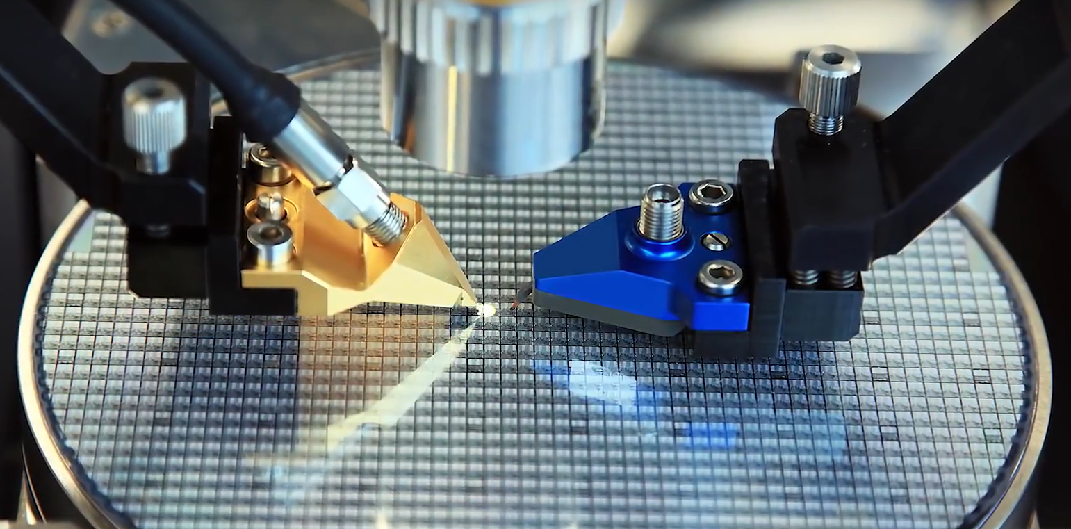
Here’s the actual patent from 1962, an invention that changed our world forever!
这个 1962 年的真实专利,永远改变了世界
Using similar steps, photolithography can create other useful electronic elements, like
用类似步骤,光刻可以制作其他电子元件 \N 比如电阻和电容,都在一片硅上
resistors and capacitors, all on a single piece of silicon
用类似步骤,光刻可以制作其他电子元件 \N 比如电阻和电容,都在一片硅上
plus all the wires needed to hook them up into circuits
而且互相连接的电路也做好了
Goodbye discrete components!
再见了,分立元件!
In our example, we made one transistor, but in the real world,
之前的例子 只做了一个晶体管,但现实中 \N 光刻法一次会做上百万个细节
photomasks lay down millions of little details all at once.
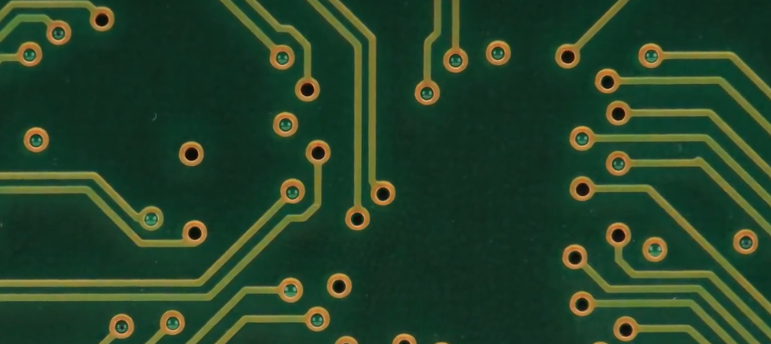
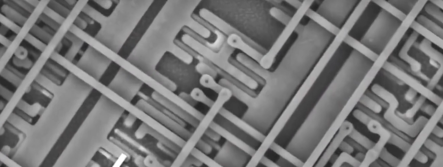
Here is what an IC might look like from above, with wires crisscrossing above and below each other,
芯片放大是这样的,导线上下交错,连接各个元件
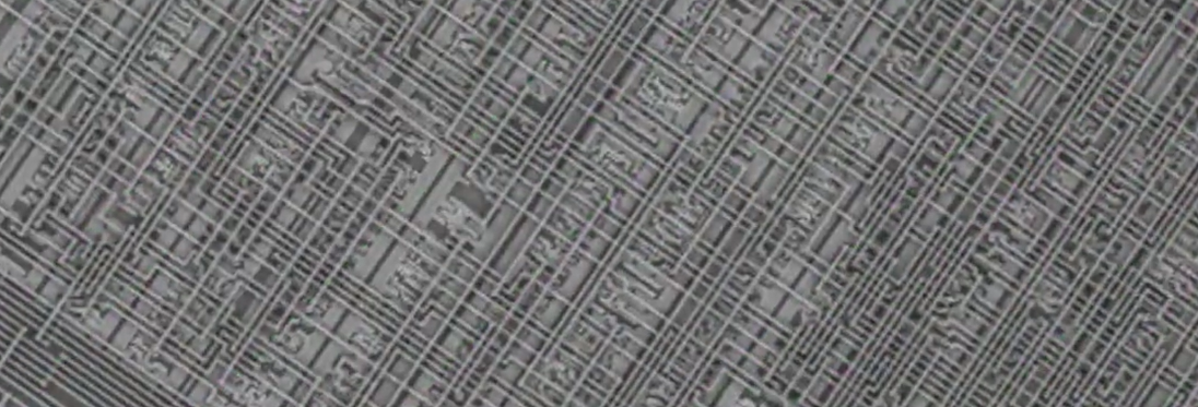
interconnecting all the individual elements together into complex circuits.
芯片放大是这样的,导线上下交错,连接各个元件
Although we could create a photomask for an entire wafer,
尽管可以把光掩膜投影到一整片晶圆上 \N 但光可以投射成任意大小
we can take advantage of the fact that light can be focused and projected to any size we want.
In the same way that a film can be projected to fill an entire movie screen,
就像投影仪可以投满荧幕一样
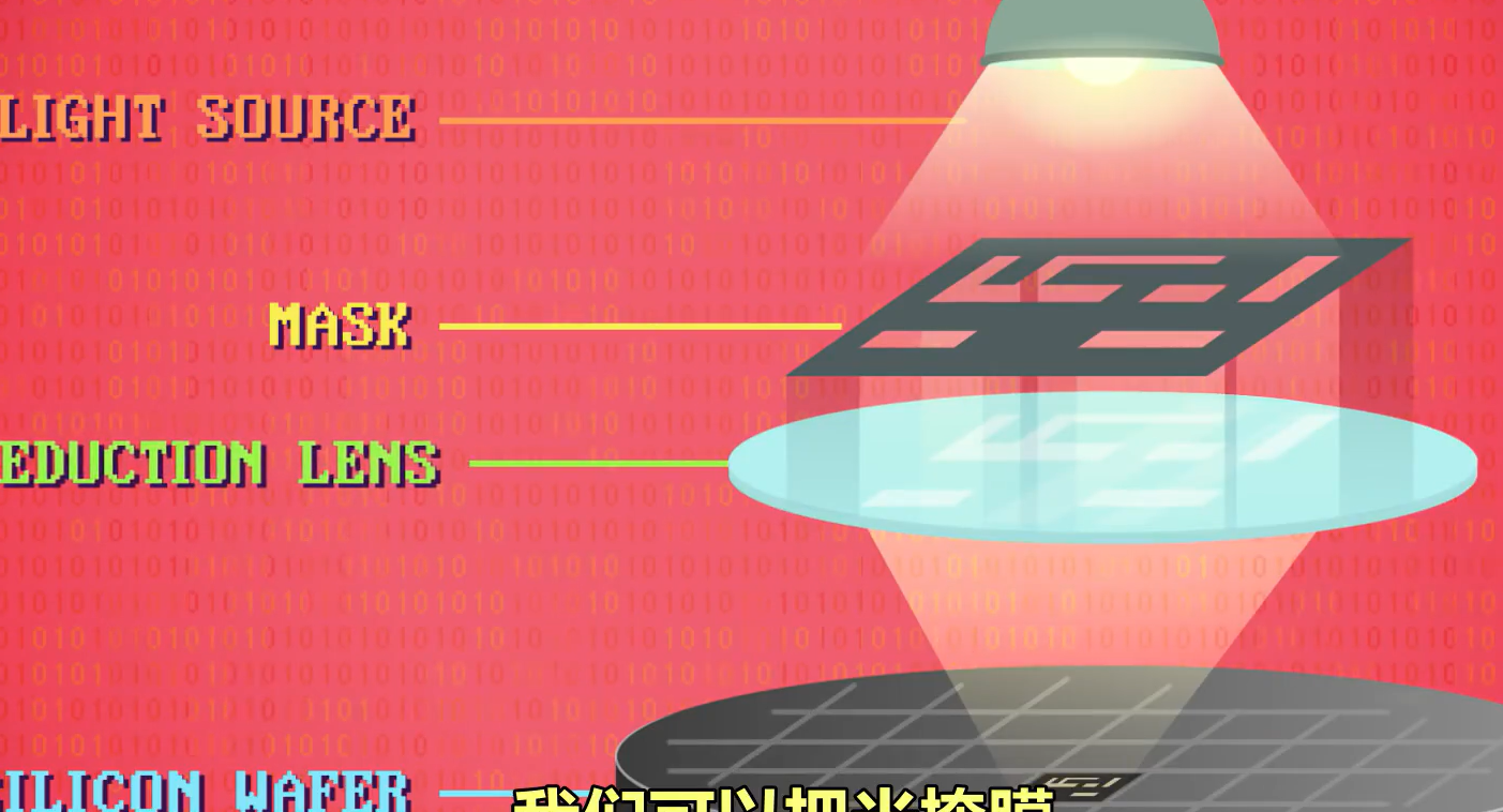
we can focus a photomask onto a very small patch of silicon, creating incredibly fine details.
我们可以把光掩膜 \N 聚焦到极小的区域,制作出非常精细的细节
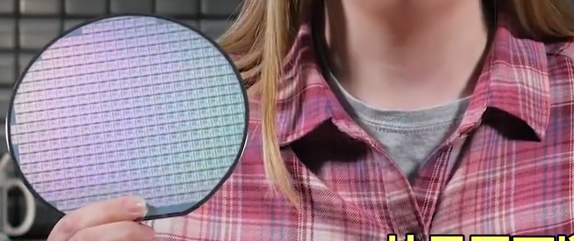
A single silicon wafer is generally used to create dozens of ICs.
一片晶圆可以做很多 IC \N 整块都做完后,可以切割然后包进微型芯片
Then, once you’ve got a whole wafer full, you cut them up and package them into microchips,
一片晶圆可以做很多 IC \N 整块都做完后,可以切割然后包进微型芯片
those little black rectangles you see in electronics all the time.
微型芯片就是在电子设备中那些小长方体
Just remember: at the heart of each of those chips is one of these small pieces of silicon.
记住,芯片的核心都是一小片 IC
As photolithography techniques improved, the size of transistors shrunk, allowing for greater densities.
随着光刻技术发展,晶体管变小 密度变高
At the start of the 1960s, an IC rarely contained more than 5 transistors,
1960 年代初,IC 很少超过 5 个晶体管,因为塞不下
they just couldn’t possibly fit.
But, by the mid 1960s, we were starting to see ICs with over 100 transistors on the market.
但 1960 年代中期 \N 市场上开始出现超过 100 个晶体管的 IC
In 1965, Gordon Moore could see the trend: that approximately every two years,
1965年,戈登·摩尔看到了趋势:每两年左右,
thanks to advances in materials and manufacturing, you could fit twice the number of transistors
得益于材料和制造技术的发展 \N 同样大小的空间,能塞进两倍数量的晶体管!
into the same amount of space.
This is called Moore’s Law.
这叫 摩尔定律
The term is a bit of a misnomer though.
然而这个名字不太对 \N 因为它不是定律,只是一种趋势
It’s not really a law at all, more of a trend.
But it’s a good one.
但它是对的
IC prices also fell dramatically, from an average of $50 in 1962 to around $2 in 1968.
芯片的价格也急剧下降 \N 1962年平均50美元,下降到1968年2美元左右
Today, you can buy ICs for cents.
如今 几美分就能买到 IC
Smaller transistors and higher densities had other benefits too.
晶体管更小密度更高 还有其他好处
The smaller the transistor, the less charge you have to move around, allowing it to switch
晶体管越小,要移动的电荷量就越少 \N 能更快切换状态 耗电更少
states faster and consume less power.
Plus, more compact circuits meant less delay in signals resulting in faster clock speeds.
电路更紧凑 还意味着信号延迟更低 \N 导致时钟速度更快
In 1968, Robert Noyce and Gordon Moore teamed up and founded a new company,
1968年,罗伯特·诺伊斯 和 戈登·摩尔 \N 联手成立了一家新公司
combining the words Integrated and Electronics…
结合 Intergrated(集成) 和 Electronics(电子) 两个词
Intel. the largest chip maker today.
取名 Intel, 如今最大的芯片制造商
The Intel 4004 CPU, from Episodes 7 and 8, was a major milestone.
Intel 4004 CPU, 在第 7, 8 集介绍过 \N 是个重要里程碑
Released in 1971, it was the first processor that shipped as an IC, what’s called a microprocessor,
发布于1971年 \N 是第一个用 IC 做的处理器,也叫微型处理器
because it was so beautifully small!
因为真的非常小!
It contained 2,300 transistors.
它有2300个晶体管
People marveled at the level of integration, an entire CPU in one chip,
人们惊叹于它的整合水平 \N 整个 CPU 在一个芯片里
which just two decades earlier would have filled an entire room using discrete components.
而仅仅 20 年前,用分立元件会占满整个屋子
This era of integrated circuits, especially microprocessors, ushered in the third generation of computing.
集成电路的出现 \N 尤其是用来做微处理器,开启了计算 3.0
And the Intel 4004 was just the start.
而 Intel 4004 只是个开始,CPU 晶体管数量爆发增长
By 1980, CPUs contained 30 thousand transistors.
1980年,3 万晶体管 \N 1990年,100 万晶体管
By 2000, 30 million transistors,
2000年,3000 万个晶体管
and by 2010, ONE. BILLION. TRANSISTORS. IN ONE. IC. OMG!
2010年,10亿个晶体管!\N 在一个芯片里!我的天啊!
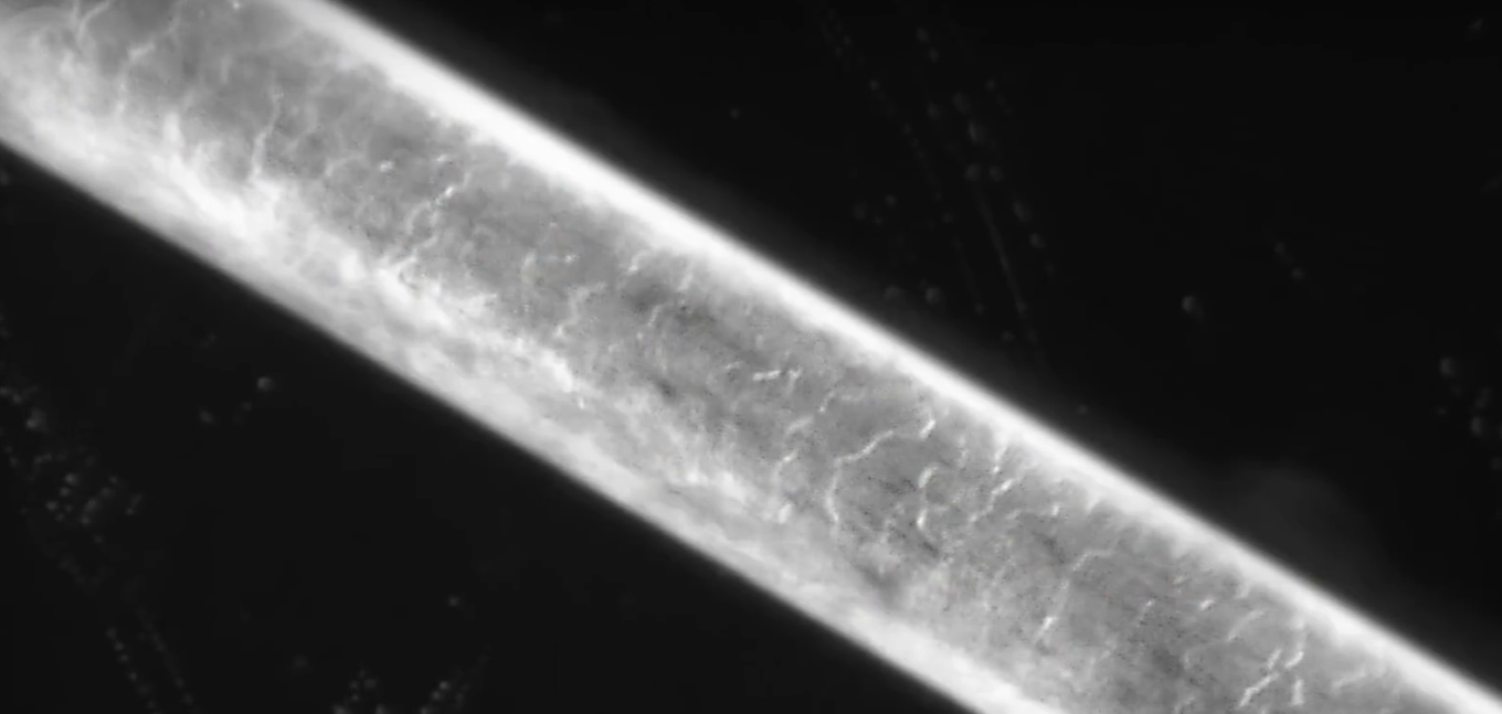
To achieve this density, the finest resolution possible with photolithography has improved
为了达到这种密度,光刻的分辨率 \N 从大约一万纳米,大概是人类头发直径的 1/10
from roughly 10 thousand nanometers, that’s about 1/10th the thickness of a human hair,
为了达到这种密度,光刻的分辨率 \N 从大约一万纳米,大概是人类头发直径的 1/10
to around 14 nanometers today.
发展到如今的 14 纳米 \N 比血红细胞小 400 倍!
That’s over 400 times smaller than a red blood cell!
发展到如今的 14 纳米 \N 比血红细胞小 400 倍!
And of course, CPU’s weren’t the only components to benefit.
当然,CPU 不是唯一受益的元件
Most electronics advanced essentially exponentially:
大多数电子器件都在指数式发展:\N 内存,显卡,固态硬盘,摄像头感光元件,等等
RAM, graphics cards, solid state hard drives, camera sensors, you name it.
大多数电子器件都在指数式发展:\N 内存,显卡,固态硬盘,摄像头感光元件,等等
Today’s processors, like the A10 CPU inside Of an iPhone 7, contains a mind melting 3.3 BILLION
如今的处理器,比如 iPhone 7 的 A10 CPU \N 有33亿个晶体管
transistors in an IC roughly 1cm by 1cm.
面积仅有 1cm x 1cm,比一张邮票还小
That’s smaller than a postage stamp!
面积仅有 1cm x 1cm,比一张邮票还小
And modern engineers aren’t laying out these designs by hand, one transistor at a time
现代工程师设计电路时,当然不是手工一个个设计晶体管 \N 这不是人力能做到的
Starting in the 1970’s, very-large-scale integration, or VLSI software, has been used
1970年代开始,超大规模集成(VLSI)软件 \N 用来自动生成芯片设计
Using techniques like logic synthesis, where whole, high-level components can be laid down,like a memory cache
用比如 “逻辑综合” 这种技术 \N 可以放一整个高级组件,比如内存缓存
the software generates the circuit in the most efficient way possible.
软件会自动生成电路,做到尽可能高效
Many consider this to be the start of fourth generation computers.
许多人认为这是计算 4.0 的开始
Unfortunately, experts have been predicting the end of Moore’s Law for decades
坏消息是,专家们几十年来 \N 一直在预言摩尔定律的终结
and we might finally be getting close to it.
现在可能终于接近了
There are two significant issues holding us back from further miniaturization.
进一步做小,会面临 2 个大问题
First, we’re bumping into limits on how fine we can make features on a photomask and
- 用光掩膜把图案弄到晶圆上 \N 因为光的波长,精度已达极限
it’s resultant wafer due to the wavelengths of light used in photolithography.
In response, scientists have been developing light sources with smaller and smaller wavelengths
所以科学家在研制波长更短的光源,投射更小的形状
that can project smaller and smaller features.
The second issue is that when transistors get really really small, where electrodes
2. 当晶体管非常小,电极之间可能只距离几个原子 \N 电子会跳过间隙,这叫:量子隧道贯穿
might be separated by only a few dozen atoms, electrons can jump the gap, a phenomenon called
quantum tunneling.
If transistors leak current, they don’t make very good switches.
如果晶体管漏电,就不是好开关
Nonetheless, scientists and engineers are hard at work figuring out ways around these problems.
科学家和工程师在努力找解决方法
Transistors as small as 1 nanometer have been demonstrated in research labs.
实验室中已造出小至1纳米的晶体管
Whether this will ever be commercially feasible remains MASKED in mystery.
能不能商业量产依然未知,未来也许能解决
But maybe we’ll be able to RESOLVE it in the future.
I’m DIEING to know. See you next week.
我非常期待!下周见!